
A solar cell or photovoltaic cell is a device that converts solar energy into electricity by the photovoltaic effect. Photovoltaics is the field of technology and research related to the application of solar cells as solar energy. Sometimes the term solar cell is reserved for devices intended specifically to capture energy from sunlight, while the term photovoltaic cell is used when the source is unspecified.
Assemblies of cells are used to make solar modules, which may in turn be linked in photovoltaic arrays.
Solar cells have many applications. Individual cells are used for powering small devices such as electronic calculators. Photovoltaic arrays generate a form of renewable electricity, particularly useful in situations where electrical power from the grid is unavailable such as in remote area power systems, Earth-orbiting satellites and space probes, remote radiotelephones and water pumping applications. Photovoltaic electricity is also increasingly deployed in grid-tied electrical systems.
[edit] History
The term "photovoltaic" comes from the Greek φώς:phos meaning "light", and "voltaic", meaning electrical, from the name of the Italian physicist Volta, after whom the measurement unit volt is named. The term "photo-voltaic" has been in use in English since 1849.[1]
The photovoltaic effect was first recognized in 1839 by French physicist Alexandre-Edmond Becquerel. However, it was not until 1883 that the first solar cell was built, by Charles Fritts, who coated the semiconductor selenium with an extremely thin layer of gold to form the junctions. The device was only around 1% efficient. Russell Ohl patented the modern solar cell in 1946 (U.S. Patent 2,402,662, "Light sensitive device"). Sven Ason Berglund had a prior patent concerning methods of increasing the capacity of photosensitive cells. The modern age of solar power technology arrived in 1954 when Bell Laboratories, experimenting with semiconductors, accidentally found that silicon doped with certain impurities was very sensitive to light.
This resulted in the production of the first practical solar cells with a sunlight energy conversion efficiency of around 6 percent. Russia launched the first artificial satellite in 1957, and the United States' first artificial satellite was launched in 1958 using solar cells created by Peter Iles in an effort spearheaded by Hoffman Electronics. The first spacecraft to use solar panels was the US satellite Explorer 1 in January 1958. This milestone created interest in producing and launching a geostationary communications satellite, in which solar energy would provide a viable power supply. This was a crucial development which stimulated funding from several governments into research for improved solar cells.
In 1970 the first highly effective GaAs heterostructure solar cells were created by Zhores Alferov and his team in the USSR. [2][3][4] Metal Organic Chemical Vapor Deposition (MOCVD, or OMCVD) production equipment was not developed until the early 1980s, limiting the ability of companies to manufacture the GaAs solar cell. In the United States, the first 17% efficient air mass zero (AM0) single-junction GaAs solar cells were manufactured in production quantities in 1988 by Applied Solar Energy Corporation (ASEC). The "dual junction" cell was accidentally produced in quantity by ASEC in 1989 as a result of the change from GaAs on GaAs substrates to GaAs on Germanium (Ge) substrates. The accidental doping of Ge with the GaAs buffer layer created higher open circuit voltages, demonstrating the potential of using the Ge substrate as another cell. As GaAs single-junction cells topped 19% AM0 production efficiency in 1993, ASEC developed the first dual junction cells for spacecraft use in the United States, with a starting efficiency of approximately 20%. These cells did not utilize the Ge as a second cell, but used another GaAs-based cell with different doping. Eventually GaAs dual junction cells reached production efficiencies of about 22%. Triple Junction solar cells began with AM0 efficiencies of approximately 24% in 2000, 26% in 2002, 28% in 2005, and in 2007 have evolved to a 30% AM0 production efficiency, currently in qualification. In 2007, two companies in the United States, Emcore Photovoltaics and Spectrolab, produce 95% of the world's 28% efficient solar cells.
Possible reference please confirm. Retrieved on 2008-05-22.The first generation photovoltaic cell consists of a large-area, single-crystal, single layer p-n junction diode, capable of generating usable electrical energy from light sources with the wavelengths of sunlight. These cells are typically made using a diffusion process with silicon wafers. First-generation photovoltaic cells (also known as silicon wafer-based solar cells) are the dominant technology in the commercial production of solar cells, accounting for more than 86% of the terrestrial solar cell market.
The second generation of photovoltaic materials is based on the use of thin epitaxial deposits of semiconductors on lattice-matched wafers. There are two classes of epitaxial photovoltaics - space and terrestrial. Space cells typically have higher AM0 efficiencies (28-30%) in production, but have a higher cost per watt. Their "thin-film" cousins have been developed using lower-cost processes, but have lower AM0 efficiencies (7-9%) in production and are questionable for space applications. The advent of thin-film technology contributed to a prediction of greatly reduced costs for thin film solar cells that has yet to be achieved. There are currently (2007) a number of technologies/semiconductor materials under investigation or in mass production. Examples include amorphous silicon, polycrystalline silicon, micro-crystalline silicon, cadmium telluride, copper indium selenide/sulfide. An advantage of thin-film technology theoretically results in reduced mass so it allows fitting panels on light or flexible materials, even textiles. The advent of thin GaAs-based films for space applications (so-called "thin cells") with potential AM0 efficiencies of up to 37% are currently in the development stage for high specific power applications. Second generation solar cells now comprise a small segment of the terrestrial photovoltaic market, and approximately 90% of the space market.
Third-generation photovoltaics are proposed to be very different from the previous semiconductor devices as they do not rely on a traditional p-n junction to separate photogenerated charge carriers. For space applications quantum well devices (quantum dots, quantum ropes, etc.) and devices incorporating carbon nanotubes are being studied - with a potential for up to 45% AM0 production efficiency. For terrestrial applications, these new devices include photoelectrochemical cells, polymer solar cells, nanocrystal solar cells, Dye-sensitized solar cells and are still in the research phase.
[edit] Applications and implementations


Solar cells are often electrically connected and encapsulated as a module. PV modules often have a sheet of glass on the front (sun up) side , allowing light to pass while protecting the semiconductor wafers from the elements (rain, hail, etc.). Solar cells are also usually connected in series in modules, creating an additive voltage. Connecting cells in parallel will yield a higher current. Modules are then interconnected, in series or parallel, or both, to create an array with the desired peak DC voltage and current.
The power output of a solar array is measured in watts or kilowatts. In order to calculate the typical energy needs of the application, a measurement in watt-hours, kilowatt-hours or kilowatt-hours per day is often used. A common rule of thumb is that average power is equal to 20% of peak power, so that each peak kilowatt of solar array output power corresponds to energy production of 4.8 kW·h per day.
To make practical use of the solar-generated energy, the electricity is most often fed into the electricity grid using inverters (grid-connected PV systems); in stand alone systems, batteries are used to store the energy that is not needed immediately.
[edit] Theory
[edit] Simple explanation
- Photons in sunlight hit the solar panel and are absorbed by semiconducting materials, such as silicon.
- Electrons (negatively charged) are knocked loose from their atoms, allowing them to flow through the material to produce electricity. The complementary positive charges that are also created (like bubbles) are called holes and flow in the direction opposite of the electrons in a silicon solar panel.
- An array of solar panels converts solar energy into a usable amount of direct current (DC) electricity.
Optionally:
- The DC current enters an inverter.
- The inverter turns DC electricity into 120 or 240-volt AC (alternating current) electricity needed for home appliances.
- The AC power enters the utility panel in the house.
- The electricity is then distributed to appliances or lights in the house.
- The electricity that is not used will be re-routed and used in other facilities.
[edit] Photogeneration of charge carriers
When a photon hits a piece of silicon, one of three things can happen:
- the photon can pass straight through the silicon — this (generally) happens for lower energy photons,
- the photon can reflect off the surface,
- the photon can be absorbed by the silicon, if the photon energy is higher than the silicon band gap value. This generates an electron-hole pair and sometimes heat, depending on the band structure.
When a photon is absorbed, its energy is given to an electron in the crystal lattice. Usually this electron is in the valence band, and is tightly bound in covalent bonds between neighboring atoms, and hence unable to move far. The energy given to it by the photon "excites" it into the conduction band, where it is free to move around within the semiconductor. The covalent bond that the electron was previously a part of now has one fewer electron — this is known as a hole. The presence of a missing covalent bond allows the bonded electrons of neighboring atoms to move into the "hole," leaving another hole behind, and in this way a hole can move through the lattice. Thus, it can be said that photons absorbed in the semiconductor create mobile electron-hole pairs.
A photon need only have greater energy than that of the band gap in order to excite an electron from the valence band into the conduction band. However, the solar frequency spectrum approximates a black body spectrum at ~6000 K, and as such, much of the solar radiation reaching the Earth is composed of photons with energies greater than the band gap of silicon. These higher energy photons will be absorbed by the solar cell, but the difference in energy between these photons and the silicon band gap is converted into heat (via lattice vibrations — called phonons) rather than into usable electrical energy.
[edit] Charge carrier separation
There are two main modes for charge carrier separation in a solar cell:
- drift of carriers, driven by an electrostatic field established across the device
- diffusion of carriers from zones of high carrier concentration to zones of low carrier concentration (following a gradient of electrochemical potential).
In the widely used p-n junction solar cells, the dominant mode of charge carrier separation is by drift. However, in non-p-n-junction solar cells (typical of the third generation of solar cell research such as dye and polymer thin-film solar cells), a general electrostatic field has been confirmed to be absent, and the dominant mode of separation is via charge carrier diffusion.[citation needed]
[edit] The p-n junction
The most commonly known solar cell is configured as a large-area p-n junction made from silicon. As a simplification, one can imagine bringing a layer of n-type silicon into direct contact with a layer of p-type silicon. In practice, p-n junctions of silicon solar cells are not made in this way, but rather, by diffusing an n-type dopant into one side of a p-type wafer (or vice versa).
If a piece of p-type silicon is placed in intimate contact with a piece of n-type silicon, then a diffusion of electrons occurs from the region of high electron concentration (the n-type side of the junction) into the region of low electron concentration (p-type side of the junction). When the electrons diffuse across the p-n junction, they recombine with holes on the p-type side. The diffusion of carriers does not happen indefinitely however, because of an electric field which is created by the imbalance of charge immediately on either side of the junction which this diffusion creates. The electric field established across the p-n junction creates a diode that promotes current to flow in only one direction across the junction. Electrons may pass from the p-type side into the n-type side, and holes may pass from the n-type side to the p-type side, but not the other way around[5]. This region where electrons have diffused across the junction is called the depletion region because it no longer contains any mobile charge carriers. It is also known as the "space charge region".
[edit] Connection to an external load
Ohmic metal-semiconductor contacts are made to both the n-type and p-type sides of the solar cell, and the electrodes connected to an external load. Electrons that are created on the n-type side, or have been "collected" by the junction and swept onto the n-type side, may travel through the wire, power the load, and continue through the wire until they reach the p-type semiconductor-metal contact. Here, they recombine with a hole that was either created as an electron-hole pair on the p-type side of the solar cell, or swept across the junction from the n-type side after being created there.
[edit] Equivalent circuit of a solar cell


To understand the electronic behavior of a solar cell, it is useful to create a model which is electrically equivalent, and is based on discrete electrical components whose behavior is well known. An ideal solar cell may be modelled by a current source in parallel with a diode; in practice no solar cell is ideal, so a shunt resistance and a series resistance component are added to the model.[6] The resulting equivalent circuit of a solar cell is shown on the left. Also shown, on the right, is the schematic representation of a solar cell for use in circuit diagrams.
[edit] Circuit Equations defining solar cell
The equations which describe the I-V characteristics of the cell are


where
- k is Boltzman's constant
- q is charge on an electron
- Vg is band gap voltage
- n is diode quality factor
- Rs is series resistance of cell
- Rsh is shunt resistance
- T1 and T2 are reference temperature in Kelvin
- T is working temperature of cell in Kelvin
- Voc is open circuit voltage
- Isc is short circuit current
- Io is reverse saturation current of diode
- I is the current through Rs
- IL is current produced by the cell
in many sources IL is also known as Iph.
[edit] Solar cell efficiency factors
[edit] Energy conversion efficiency
A solar cell's energy conversion efficiency (η, "eta"), is the percentage of power converted (from absorbed light to electrical energy) and collected, when a solar cell is connected to an electrical circuit. This term is calculated using the ratio of the maximum power point, Pm, divided by the input light irradiance (E, in W/m²) under standard test conditions (STC) and the surface area of the solar cell (Ac in m²).

STC specifies a temperature of 25°C and an irradiance of 1000 W/m² with an air mass 1.5 (AM1.5) spectrum. These correspond to the irradiance and spectrum of sunlight incident on a clear day upon a sun-facing 37°-tilted surface with the sun at an angle of 41.81° above the horizon.[7][8] This condition approximately represents solar noon near the spring and autumn equinoxes in the continental United States with surface of the cell aimed directly at the sun. Thus, under these conditions a solar cell of 12% efficiency with a 100 cm2 (0.01 m2) surface area can be expected to produce approximately 1.2 watts of power.
The losses of a solar cell may be broken down into reflectance losses, thermodynamic efficiency, recombination losses and resistive electrical loss. The overall efficiency is the product of each of these individual losses.
Due to the difficulty in measuring these parameters directly, other parameters are measured instead: Thermodynamic Efficiency, Quantum Efficiency, VOC ratio, and Fill Factor. Reflectance losses are a portion of the Quantum Efficiency under "External Quantum Efficiency". Recombination losses make up a portion of the Quantum Efficiency, VOC ratio, and Fill Factor. Resistive losses are predominantly categorized under Fill Factor, but also make up minor portions of the Quantum Efficiency, VOC ratio.
[edit] Thermodynamic Efficiency Limit
Solar cells operate as quantum energy conversion devices, and are therefore subject to the "Thermodynamic Efficiency Limit". Photons with an energy below the band gap of the absorber material cannot generate a hole-electron pair, and so their energy is not converted to useful output and only generates heat if absorbed. For photons with an energy above the band gap energy, only a fraction of the energy above the band gap can be converted to useful output. When a photon of greater energy is absorbed, the excess energy above the band gap is converted to kinetic energy of the carrier combination. The excess kinetic energy is converted to heat through phonon interactions as the kinetic energy of the carriers slows to equilibrium velocity.
Solar cells with multiple band gap absorber materials are able to more efficiently convert the solar spectrum. By using multiple band gaps, the solar spectrum may be broken down into smaller bins where the thermodynamic efficiency limit is higher for each bin.[9]
[edit] Quantum efficiency
As described above, when a photon is absorbed by a solar cell it is converted to an electron-hole pair. This electron-hole pair may then travel to the surface of the solar cell and contribute to the current produced by the cell; such a carrier is said to be collected. Alternatively, the carrier may give up its energy and once again become bound to an atom within the solar cell without reaching the surface; this is called recombination, and carriers that recombine do not contribute to the production of electrical current.
Quantum efficiency refers to the percentage of photons that are converted to electric current (i.e., collected carriers) when the cell is operated under short circuit conditions. External quantum efficiency is the fraction of incident photons that are converted to electrical current, while internal quantum efficiency is the fraction of absorbed photons that are converted to electrical current. Mathematically, internal quantum efficiency is related to external quantum efficiency by the reflectance of the solar cell; given a perfect anti-reflection coating, they are the same.
Quantum efficiency should not be confused with energy conversion efficiency, as it does not convey information about the power collected from the solar cell. Furthermore, quantum efficiency is most usefully expressed as a spectral measurement (that is, as a function of photon wavelength or energy). Since some wavelengths are absorbed more effectively than others in most semiconductors, spectral measurements of quantum efficiency can yield information about which parts of a particular solar cell design are most in need of improvement.
[edit] VOC ratio
Due to recombination, the open circuit voltage (VOC) of the cell will be below the band gap voltage of the cell. Since the energy of the photons must be at or above the band gap to generate a carrier pair, cell voltage below the band gap voltage represents a loss. This loss is represented by the ratio of VOC divided by VG
[edit] Maximum-power point
A solar cell may operate over a wide range of voltages (V) and currents (I). By increasing the resistive load on an irradiated cell continuously from zero (a short circuit) to a very high value (an open circuit) one can determine the maximum-power point, the point that maximizes V×I; that is, the load for which the cell can deliver maximum electrical power at that level of irradiation. (The output power is zero in both the short circuit and open circuit extremes).
A high quality, monocrystalline silicon solar cell, at 25 °C cell temperature, may produce 0.60 volts open-circuit (Voc). The cell temperature in full sunlight, even with 25 °C air temperature, will probably be close to 45 °C, reducing the open-circuit voltage to 0.55 volts per cell. The voltage drops modestly, with this type of cell, until the short-circuit current is approached (Isc). Maximum power (with 45 °C cell temperature) is typically produced with 75% to 80% of the open-circuit voltage (0.43 volts in this case) and 90% of the short-circuit current. This output can be up to 70% of the Voc x Isc product. The short-circuit current (Isc) from a cell is nearly proportional to the illumination, while the open-circuit voltage (Voc) may drop only 10% with a 80% drop in illumination. Lower-quality cells have a more rapid drop in voltage with increasing current and could produce only 1/2 Voc at 1/2 Isc. The usable power output could thus drop from 70% of the Voc x Isc product to 50% or even as little as 25%. Vendors who rate their solar cell "power" only as Voc x Isc, without giving load curves, can be seriously distorting their actual performance.
The maximum power point of a photovoltaic varies with incident illumination. For systems large enough to justify the extra expense, a maximum power point tracker tracks the instantaneous power by continually measuring the voltage and current (and hence, power transfer), and uses this information to dynamically adjust the load so the maximum power is always transferred, regardless of the variation in lighting.
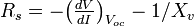
[edit] Fill factor
Another defining term in the overall behavior of a solar cell is the fill factor (FF). This is the ratio of the maximum power point divided by the open circuit voltage (Voc) and the short circuit current (Isc):

[edit] Comparison of energy conversion efficiencies
At this point, discussion of the different ways to calculate efficiency for space cells and terrestrial cells is necessary to alleviate confusion. In space, where there is no atmosphere, the spectrum of the sun is relatively unfiltered. However on earth, with air filtering the incoming light, the solar spectrum changes. To account for the spectral differences, a system was devised to calculate this filtering effect. Simply, the filtering effect ranges from Air Mass 0 in space, to approximately Air Mass 1.5 on earth. Multiplying the spectral differences by the quantum efficiency of the solar cell in question will yield the efficiency of the device. For example, a Silicon solar cell in space might have an efficiency of 14% at AM0, but have an efficiency of 16% on earth at AM 1.5. Terrestrial efficiencies typically are greater than space efficiencies.
Solar cell efficiencies vary from 6% for amorphous silicon-based solar cells to 40.7% with multiple-junction research lab cells and 42.8% with multiple dies assembled into a hybrid package.[10] Solar cell energy conversion efficiencies for commercially available multicrystalline Si solar cells are around 14-19%[11]. The highest efficiency cells have not always been the most economical — for example a 30% efficient multijunction cell based on exotic materials such as gallium arsenide or indium selenide and produced in low volume might well cost one hundred times as much as an 8% efficient amorphous silicon cell in mass production, while only delivering about four times the electrical power.
However, there is a way to "boost" solar power. By increasing the light intensity, typically photogenerated carriers are increased, resulting in increased efficiency by up to 15%. These so-called "concentrator systems" have only begun to become cost-competitive as a result of the development of high efficiency GaAs cells. The increase in intensity is typically accomplished by using concentrating optics. A typical concentrator system may use a light intensity 6-400 times the sun, and increase the efficiency of a one sun GaAs cell from 31% at AM 1.5 to 35%.
A common method used to express economic costs of electricity-generating systems is to calculate a price per delivered kilowatt-hour (kWh). The solar cell efficiency in combination with the available irradiation has a major influence on the costs, but generally speaking the overall system efficiency is important. Using the commercially available solar cells (as of 2006) and system technology leads to system efficiencies between 5 and 19%. As of 2005, photovoltaic electricity generation costs ranged from ~0.60 US$/kWh (0.50 €/kWh) (central Europe) down to ~0.30 US$/kWh (0.25 €/kWh) in regions of high solar irradiation. This electricity is generally fed into the electrical grid on the customer's side of the meter. The cost can be compared to prevailing retail electric pricing (as of 2005), which varied from between 0.04 and 0.50 US$/kWh worldwide. (Note: in addition to solar irradiance profiles, these costs/kwh calculations will vary depending on assumptions for years of useful life of a system. Most c-Si panels are warrantied for 25 years and should see 35+ years of useful life.)
The chart at the right illustrates the various commercial large-area module energy conversion efficiencies and the best laboratory efficiencies obtained for various materials and technologies.

[edit] Watts peak
Since solar cell output power depends on multiple factors, such as the sun's incidence angle, for comparison purposes between different cells and panels, the measure of watts peak (Wp) is used. It is the output power under these conditions known as STC:[12][13]
- insolation (solar irradiance) 1000 W/m²
- solar reference spectrum AM (airmass) 1.5
- cell temperature 25°C
[edit] Solar cells and energy payback
In the 1990s, when silicon cells were twice as thick, efficiencies were 30% lower than today and lifetimes were shorter, it may well have cost more energy to make a cell than it could generate in a lifetime. In the meantime, the technology has progressed significantly, and the energy payback time of a modern photovoltaic module is typically from 1 to 4 years [14] depending on the type and where it is used (see net energy gain). With a typical lifetime of 20 to 30 years, this means that modern solar cells are net energy producers, i.e they generate much more energy over their lifetime than the energy expended in producing them.[15][14][16]
[edit] Light-absorbing materials
All solar cells require a light absorbing material contained within the cell structure to absorb photons and generate electrons via the photovoltaic effect. The materials used in solar cells tend to have the property of preferentially absorbing the wavelengths of solar light that reach the earth surface; however, some solar cells are optimized for light absorption beyond Earth's atmosphere as well. Light absorbing materials can often be used in multiple physical configurations to take advantage of different light absorption and charge separation mechanisms. Many currently available solar cells are configured as bulk materials that are subsequently cut into wafers and treated in a "top-down" method of synthesis (silicon being the most prevalent bulk material). Other materials are configured as thin-films (inorganic layers, organic dyes, and organic polymers) that are deposited on supporting substrates, while a third group are configured as nanocrystals and used as quantum dots (electron-confined nanoparticles) embedded in a supporting matrix in a "bottom-up" approach. Silicon remains the only material that is well-researched in both bulk and thin-film configurations. The following is a current list of light absorbing materials, listed by configuration and substance-name:
[edit] Bulk
These bulk technologies are often referred to as wafer-based manufacturing. In other words, in each of these approaches, self-supporting wafers between 180 to 240 micrometers thick are processed and then soldered together to form a solar cell module. A general description of silicon wafer processing is provided in Manufacture and Devices.
[edit] Silicon

By far, the most prevalent bulk material for solar cells is crystalline silicon (abbreviated as a group as c-Si), also known as "solar grade silicon". Bulk silicon is separated into multiple categories according to crystallinity and crystal size in the resulting ingot, ribbon, or wafer.
- monocrystalline silicon (c-Si): often made using the Czochralski process. Single-crystal wafer cells tend to be expensive, and because they are cut from cylindrical ingots, do not completely cover a square solar cell module without a substantial waste of refined silicon. Hence most c-Si panels have uncovered gaps at the four corners of the cells.
- Poly- or multicrystalline silicon (poly-Si or mc-Si): made from cast square ingots — large blocks of molten silicon carefully cooled and solidified. These cells are less expensive to produce than single crystal cells but are less efficient.
- Ribbon silicon: formed by drawing flat thin films from molten silicon and having a multicrystalline structure. These cells have lower efficiencies than poly-Si, but save on production costs due to a great reduction in silicon waste, as this approach does not require sawing from ingots.
[edit] Thin films
The various thin-film technologies currently being developed reduce the amount (or mass) of light absorbing material required in creating a solar cell. This can lead to reduced processing costs from that of bulk materials (in the case of silicon thin films) but also tends to reduce energy conversion efficiency, although many multi-layer thin films have efficiencies above those of bulk silicon wafers.
[edit] CdTe
Cadmium telluride is an efficient light-absorbing material for thin-film solar cells. Compared to other thin-film materials, CdTe is easier to deposit and more suitable for large-scale production. Despite much discussion of the toxicity of CdTe-based solar cells, this is the only technology (apart from amorphous silicon) that can be delivered on a large scale[citation needed]. The perception of the toxicity of CdTe is based on the toxicity of elemental cadmium, a heavy metal that is a cumulative poison. However it has been shown that the release of cadmium to the atmosphere is lower with CdTe-based solar cells than with silicon photovoltaics and other thin-film solar cell technologies. [17]
[edit] Copper-Indium Selenide
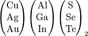 Possible combinations of I III VI elements in the periodic table that have photovoltaic effect |
The materials based on CuInSe2 that are of interest for photovoltaic applications include several elements from groups I, III and VI in the periodic table. These semiconductors are especially attractive for thin film solar cell application because of their high optical absorption coefficients and versatile optical and electrical characteristics which can in principle be manipulated and tuned for a specific need in a given device. CIS is an abbreviation for general chalcopyrite films of copper indium selenide (CuInSe2), CIGS mentioned below is a variation of CIS. CIS films (no Ga) achieved greater than 14% efficiency.[18] However, manufacturing costs of CIS solar cells at present are high when compared with amorphous silicon solar cells but continuing work is leading to more cost-effective production processes. The first large-scale production of CIS modules was started in 2006 in Germany by Wuerth Solar.
When gallium is substituted for some of the indium in CIS, the material is sometimes called CIGS , or copper indium/gallium diselenide, a solid mixture of the semiconductors CuInSe2 and CuGaSe2, often abbreviated by the chemical formula CuInxGa(1-x)Se2. Unlike the conventional silicon based solar cell, which can be modelled as a simple p-n junction (see under semiconductor), these cells are best described by a more complex heterojunction model. The best efficiency of a thin-film solar cell as of March 2008 was 19.9% with CIGS absorber layer.[19] Higher efficiencies (around 30%) can be obtained by using optics to concentrate the incident light. The use of gallium increases the optical bandgap of the CIGS layer as compared to pure CIS, thus increasing the open-circuit voltage. In another point of view, gallium is added to replace as much indium as possible due to gallium's relative availability to indium. Approximately 70%[20] of indium currently produced is used by the flat-screen monitor industry. Some investors in solar technology worry that production of CIGS cells will be limited by the availability of indium. Producing 2 GW of CIGS cells (roughly the amount of silicon cells produced in 2006) would use about 10% of the indium produced in 2004.[21] For comparison, silicon solar cells used up 33% of the world's electronic grade silicon production in 2006. Nanosolar claims to waste only 5% of the indium it uses. As of 2006, the best conversion efficiency for flexible CIGS cells on polyimide is 14.1% by Tiwari et al, at the ETH, Switzerland.
That being said, indium can easily be recycled from decommissioned PV modules. The recycling program in Germany would be is an example that highlights the regenerative industrial paradigm: "From cradle to cradle".
Selenium allows for better uniformity across the layer and so the number of recombination sites in the film are reduced which benefits the quantum efficiency and thus the conversion efficiency.[citation needed]
[edit] Gallium arsenide (GaAs) multijunction
High-efficiency cells have been developed for special applications such as satellites and space exploration. These multijunction cells consist of multiple thin films produced using molecular beam epitaxy. A triple-junction cell, for example, may consist of the semiconductors: GaAs, Ge, and GaInP2.[22] Each type of semiconductor will have a characteristic band gap energy which, loosely speaking, causes it to absorb light most efficiently at a certain color, or more precisely, to absorb electromagnetic radiation over a portion of the spectrum. The semiconductors are carefully chosen to absorb nearly all of the solar spectrum, thus generating electricity from as much of the solar energy as possible.
GaAs multijunction devices are the most efficient solar cells to date, reaching a record high of 40.7% efficiency under solar concentration and laboratory conditions.[23] These devices use 20 to 30 different semiconductors layered in series.
This technology is currently being utilised in the Mars rover missions.
Solar arrays made with a material which contains gallium arsenide GaAs and germanium Ge is seeing demand rapidly rise. In just the past 12 months (12/2006 - 12/2007), the cost of 4N gallium metal has risen from about $350 per kg to $680 per kg. Additionally, germanium metal prices have risen substantially to $1000-$1200 per kg this year. Although some Chinese producers of these materials may be able to offset some of the price increases with their lower labor costs. Those materials include gallium (4N, 6N and 7N Ga), arsenic (4N, 6N and 7N) and germanium, pyrolitic boron nitride (pBN) crucibles for growing crystals, and boron oxide, these products are critical to the entire substrate manufacturing industry.
Triple-junction GaAs solar cells were also being used as the power source of the Dutch four-time World Solar Challenge winners Nuna in 2005 and 2007.
[edit] Light-absorbing dyes
Typically a ruthenium metalorganic dye (Ru-centered) is used as a monolayer of light-absorbing material. The dye-sensitized solar cell depends on a mesoporous layer of nanoparticulate titanium dioxide to greatly amplify the surface area (200-300 m²/g TiO2, as compared to approximately 10 m²/g of flat single crystal). The photogenerated electrons from the light absorbing dye are passed on to the n-type TiO2, and the holes are passed to an electrolyte on the other side of the dye. The circuit is completed by a redox couple in the electrolyte, which can be liquid or solid. This type of cell allows a more flexible use of materials, and is typically manufactured by screen printing, with the potential for lower processing costs than those used for bulk solar cells. However, the dyes in these cells also suffer from degradation under heat and UV light, and the cell casing is difficult to seal due to the solvents used in assembly. In spite of the above, this is a popular emerging technology with some commercial impact forecast within this decade.
[edit] Organic/polymer solar cells
Organic solar cells and Polymer solar cells are built from thin films (typically 100 nm) of organic semiconductors such as polymers and small-molecule compounds like polyphenylene vinylene, copper phthalocyanine (a blue or green organic pigment) and carbon fullerenes. Energy conversion efficiencies achieved to date using conductive polymers are low at 6% efficiency[24] for the best cells to date. However, these cells could be beneficial for some applications where mechanical flexibility and disposability are important.
[edit] Silicon
Silicon thin-films are mainly deposited by chemical vapor deposition (typically plasma-enhanced (PE-CVD)) from silane gas and hydrogen gas. Depending on the deposition's parameters, this can yield:
- Amorphous silicon (a-Si or a-Si:H)
- protocrystalline silicon or
- Nanocrystalline silicon (nc-Si or nc-Si:H).
These types of silicon present dangling and twisted bonds, which results in deep defects (energy levels in the bandgap) as well as deformation of the valence and conduction bands (band tails). The solar cells made from these materials tend to have lower energy conversion efficiency than bulk silicon, but are also less expensive to produce. The quantum efficiency of thin film solar cells is also lower due to reduced number of collected charge carriers per incident photon.
Amorphous silicon has a higher bandgap (1.7 eV) than crystalline silicon (c-Si) (1.1 eV), which means it absorbs the visible part of the solar spectrum more strongly than the infrared portion of the spectrum. As nc-Si has about the same bandgap as c-Si, the two material can be combined in thin layers, creating a layered cell called a tandem cell. The top cell in a-Si absorbs the visible light and leaves the infrared part of the spectrum for the bottom cell in nanocrystalline Si.
Recently, solutions to overcome the limitations of thin-film crystalline silicon have been developed. Light trapping schemes where the incoming light is obliquely coupled into the silicon and the light traverses the film several times enhance the absorption of sunlight in the films. Thermal processing techniques enhance the crystallinity of the silicon and pacify electronic defects.[citation needed]
A silicon thin film technology is being developed for building integrated photovoltaics (BIPV) in the form of semi-transparent solar cells which can be applied as window glazing. These cells function as window tinting while generating electricity.
[edit] Nanocrystalline solar cells
These structures make use of some of the same thin-film light absorbing materials but are overlain as an extremely thin absorber on a supporting matrix of conductive polymer or mesoporous metal oxide having a very high surface area to increase internal reflections (and hence increase the probability of light absorption).
[edit] Concentrating photovoltaics (CPV)
Concentrating photovoltaic systems use a large area of lenses or mirrors to focus sunlight on a small area of photovoltaic cells.[25] If these systems use single or dual-axis tracking to improve performance, they may be referred to as Heliostat Concentrator Photovoltaics (HCPV). The primary attraction of CPV systems is their reduced usage of semiconducting material which is expensive and currently in short supply. Additionally, increasing the concentration ratio improves the performance of general photovoltaic materials[26]. Despite the advantages of CPV technologies their application has been limited by the costs of focusing, tracking and cooling equipment. On October 25, 2006, the Australian federal government and the Victorian state government together with photovoltaic technology company Solar Systems announced a project using this technology, Solar power station in Victoria, planned to come online in 2008 and be completed by 2013. This plant, at 154 MW, would be ten times larger than the largest current photovoltaic plant in the world.[27]
[edit] Silicon solar cell device manufacture

Because solar cells are semiconductor devices, they share many of the same processing and manufacturing techniques as other semiconductor devices such as computer and memory chips. However, the stringent requirements for cleanliness and quality control of semiconductor fabrication are a little more relaxed for solar cells. Most large-scale commercial solar cell factories today make screen printed poly-crystalline silicon solar cells. Single crystalline wafers which are used in the semiconductor industry can be made into excellent high efficiency solar cells, but they are generally considered to be too expensive for large-scale mass production.
Poly-crystalline silicon wafers are made by wire-sawing block-cast silicon ingots into very thin (180 to 350 micrometer) slices or wafers. The wafers are usually lightly p-type doped. To make a solar cell from the wafer, a surface diffusion of n-type dopants is performed on the front side of the wafer. This forms a p-n junction a few hundred nanometers below the surface.
Antireflection coatings, which increase the amount of light coupled into the solar cell, are typically next applied. Over the past decade, silicon nitride has gradually replaced titanium dioxide as the antireflection coating of choice because of its excellent surface passivation qualities (i.e., it prevents carrier recombination at the surface of the solar cell). It is typically applied in a layer several hundred nanometers thick using plasma-enhanced chemical vapor deposition (PECVD). Some solar cells have textured front surfaces that, like antireflection coatings, serve to increase the amount of light coupled into the cell. Such surfaces can usually only be formed on single-crystal silicon, though in recent years methods of forming them on multicrystalline silicon have been developed.
The wafer then has a full area metal contact made on the back surface, and a grid-like metal contact made up of fine "fingers" and larger "busbars" are screen-printed onto the front surface using a silver paste. The rear contact is also formed by screen-printing a metal paste, typically aluminium. Usually this contact covers the entire rear side of the cell, though in some cell designs it is printed in a grid pattern. The paste is then fired at several hundred degrees Celsius to form metal electrodes in ohmic contact with the silicon. After the metal contacts are made, the solar cells are interconnected in series (and/or parallel) by flat wires or metal ribbons, and assembled into modules or "solar panels". Solar panels have a sheet of tempered glass on the front, and a polymer encapsulation on the back. Tempered glass cannot be used with amorphous silicon cells because of the high temperatures during the deposition process.
[edit] Current research on materials and devices
- See also: Timeline of solar cells
There are currently many research groups active in the field of photovoltaics in universities and research institutions around the world. This research can be divided into three areas: making current technology solar cells cheaper and/or more efficient to effectively compete with other energy sources; developing new technologies based on new solar cell architectural designs; and developing new materials to serve as light absorbers and charge carriers.
[edit] Silicon processing
One way of reducing the cost is to develop cheaper methods of obtaining silicon that is sufficiently pure. Silicon is a very common element, but is normally bound in silica, or silica sand. Processing silica (SiO2) to produce silicon is a very high energy process - at current efficiencies, it takes over two years for a conventional solar cell to generate as much energy as was used to make the silicon it contains.[28] More energy efficient methods of synthesis are not only beneficial to the solar industry, but also to industries surrounding silicon technology as a whole.
The current industrial production of silicon is via the reaction between carbon (charcoal) and silica at a temperature around 1700 degrees Celsius. In this process, known as carbothermic reduction, each tonne of silicon (metallurgical grade, about 98% pure) is produced with the emission of about 1.5 tonnes of carbon dioxide.
Solid silica can be directly converted (reduced) to pure silicon by electrolysis in a molten salt bath at a fairly mild temperature (800 to 900 degrees Celsius).[29][30] While this new process is in principle the same as the FFC Cambridge Process which was first discovered in late 1996, the interesting laboratory finding is that such electrolytic silicon is in the form of porous silicon which turns readily into a fine powder, (with a particle size of a few micrometres), and may therefore offer new opportunities for development of solar cell technologies.
Another approach is also to reduce the amount of silicon used and thus cost, is by micromachining wafers into very thin, virtually transparent layers that could be used as transparent architectural coverings.[31] . The technique involves taking a silicon wafer, typically 1 to 2 mm thick, and making a multitude of parallel, transverse slices across the wafer, creating a large number of slivers that have a thickness of 50 micrometres and a width equal to the thickness of the original wafer. These slices are rotated 90 degrees, so that the surfaces corresponding to the faces of the original wafer become the edges of the slivers. The result is to convert, for example, a 150 mm diameter, 2 mm-thick wafer having an exposed silicon surface area of about 175 cm² per side into about 1000 slivers having dimensions of 100 mm x 2 mm x 0.1 mm, yielding a total exposed silicon surface area of about 2000 cm² per side. As a result of this rotation, the electrical doping and contacts that were on the face of the wafer are located the edges of the sliver, rather than the front and rear as is the case with conventional wafer cells. This has the interesting effect of making the cell sensitive from both the front and rear of the cell (a property known as bifaciality).[32] Using this technique, one silicon wafer is enough to build a 140 watt panel, compared to about 60 wafers needed for conventional modules of same power output.
[edit] Thin-film processing
Thin-film solar cells use less than 1% of the raw material (silicon or other light absorbers) compared to wafer based solar cells, leading to a significant price drop per kWh. There are many research groups around the world actively researching different thin-film approaches and/or materials, however it remains to be seen[vague] if these solutions can generate the same space-efficiency as traditional silicon processing.
One particularly promising technology is crystalline silicon thin films on glass substrates. This technology makes use of the advantages of crystalline silicon as a solar cell material, with the cost savings of using a thin-film approach.[citation needed]
Another interesting aspect of thin-film solar cells is the possibility to deposit the cells on all kind of materials, including flexible substrates (PET for example), which opens a new dimension for new applications.[citation needed]
[edit] Polymer processing
The invention of conductive polymers (for which Alan Heeger, Alan G. MacDiarmid and Hideki Shirakawa were awarded a Nobel prize) may lead to the development of much cheaper cells that are based on inexpensive plastics. However, all organic solar cells made to date suffer from degradation upon exposure to UV light, and hence have lifetimes which are far too short to be viable. The conjugated double bond systems in the polymers, which carry the charge, are always susceptible to breaking up when radiated with shorter wavelengths. Additionally, most conductive polymers, being highly unsaturated and reactive, are highly sensitive to atmospheric moisture and oxidation, making commercial applications difficult.
[edit] Nanoparticle processing
Experimental non-silicon solar panels can be made of quantum heterostructures, eg. carbon nanotubes or quantum dots, embedded in conductive polymers or mesoporous metal oxides. In addition, thin films of many of these materials on conventional silicon solar cells can increase the optical coupling efficiency into the silicon cell, thus boosting the overall efficiency. By varying the size of the quantum dots, the cells can be tuned to absorb different wavelengths. Although the research is still in its infancy, quantum dot-modified photovoltaics may be able to achieve up to 42 percent energy conversion efficiency due to multiple exciton generation(MEG).[33]
[edit] Transparent conductors
Many new solar cells use transparent thin films that are also conductors of electrical charge. The dominant conductive thin films used in research now are transparent conductive oxides (abbreviated "TCO"), and include fluorine-doped tin oxide (SnO2:F, or "FTO"), doped zinc oxide (e.g.: ZnO:Al), and indium tin oxide (abbreviated "ITO"). These conductive films are also used in the LCD industry for flat panel displays. The dual function of a TCO allows light to pass through a substrate window to the active light absorbing material beneath, and also serves as an ohmic contact to transport photogenerated charge carriers away from that light absorbing material. The present TCO materials are effective for research, but perhaps are not yet optimized for large-scale photovoltaic production. They require very special deposition conditions at high vacuum, they can sometimes suffer from poor mechanical strength, and most have poor transmittance in the infrared portion of the spectrum (e.g.: ITO thin films can also be used as infrared filters in airplane windows). These factors make large-scale manufacturing more costly.
A relatively new area has emerged using carbon nanotube networks as a transparent conductor for organic solar cells. Nanotube networks are flexible and can be deposited on surfaces a variety of ways. With some treatment, nanotube films can be highly transparent in the infrared, possibly enabling efficient low bandgap solar cells. Nanotube networks are p-type conductors, whereas traditional transparent conductors are exclusively n-type. The availability of a p-type transparent conductor could lead to new cell designs that simplify manufacturing and improve efficiency.
[edit] Silicon wafer based solar cells
Despite the numerous attempts at making better solar cells by using new and exotic materials, the reality is that the photovoltaics market is still dominated by silicon wafer-based solar cells (first-generation solar cells). This means that most solar cell manufacturers are equipped to produce these type of solar cells. Therefore, a large body of research is currently being done all over the world to create silicon wafer-based solar cells that can achieve higher conversion efficiency without an exorbitant increase in production cost. The aim of the research is to achieve the lowest cost per watt solar cell design that is suitable for commercial production.[vague]
[edit] Manufacturers
Solar cells are manufactured primarily in Japan, Germany, USA, and China, though numerous other nations have or are acquiring significant solar cell production capacity. While technologies are constantly evolving toward higher efficiencies, the most effective cells for low cost electrical production are not necessarily those with the highest efficiency, but those with a balance between low-cost production and efficiency high enough to minimize area-related balance of systems cost. Those companies with large scale manufacturing technology for coating inexpensive substrates may, in fact, ultimately be the lowest cost net electricity producers, even with cell efficiencies that are lower than those of single-crystal technologies.
歡迎來到Bewise Inc.的世界,首先恭喜您來到這接受新的資訊讓產業更有競爭力,我們是提供專業刀具製造商,應對客戶高品質的刀具需求,我們可以協助客戶滿足您對產業的不同要求,我們有能力達到非常卓越的客戶需求品質,這是現有相關技術無法比擬的,我們成功的滿足了各行各業的要求,包括:精密HSS DIN切削刀具、協助客戶設計刀具流程、DIN or JIS 鎢鋼切削刀具設計、NAS986 NAS965 NAS897 NAS937orNAS907 航太切削刀具,NAS航太刀具設計、超高硬度的切削刀具、BW捨棄式鑽石V卡刀’BW捨棄式金屬圓鋸片、木工捨棄式金屬圓鋸片、PCD木工圓鋸片、醫療配件刀具設計、汽車業刀具設計、電子產業鑽石刀具、全鎢鋼V卡刀-電路版專用’全鎢鋼鋸片、焊刃式側銑刀、焊刃式千鳥側銑刀、焊刃式T型銑刀、焊刃式千鳥T型銑刀、焊刃式螺旋機械鉸刀、全鎢鋼斜邊刀電路版專用、鎢鋼焊刃式高速鉸刀、超微粒鎢鋼機械鉸刀、超微粒鎢鋼定點鑽、焊刃式帶柄角度銑刀、焊刃式螺旋立銑刀、焊刃式帶柄倒角銑刀、焊刃式角度銑刀、焊刃式筒型平面銑刀、木工產業鑽石刀具等等。我們的產品涵蓋了從民生刀具到工業級的刀具設計;從微細刀具到大型刀具;從小型生產到大型量產;全自動整合;我們的技術可提供您連續生產的效能,我們整體的服務及卓越的技術,恭迎您親自體驗!!
BW Bewise Inc. Willy Chen willy@tool-tool.com bw@tool-tool.com www.tool-tool.com skype:willy_chen_bw mobile:0937-618-190 Head &Administration Office No.13,Shiang Shang 2nd St., West Chiu Taichung,Taiwan 40356 http://www.tool-tool..com / FAX:+886 4 2471 4839 N.Branch 5F,No.460,Fu Shin North Rd.,Taipei,Taiwan S.Branch No.24,Sec.1,Chia Pu East Rd.,Taipao City,Chiayi Hsien,Taiwan
Welcome to BW tool world! We are an experienced tool maker specialized in cutting tools. We focus on what you need and endeavor to research the best cutter to satisfy users’ demand. Our customers involve wide range of industries, like mold & die, aerospace, electronic, machinery, etc. We are professional expert in cutting field. We would like to solve every problem from you. Please feel free to contact us, its our pleasure to serve for you. BW product including: cutting tool、aerospace tool .HSS DIN Cutting tool、Carbide end mills、Carbide cutting tool、NAS Cutting tool、NAS986 NAS965 NAS897 NAS937orNAS907 Cutting Tools,Carbide end mill、disc milling cutter,Aerospace cutting tool、hss drill’Фрезеры’Carbide drill、High speed steel、Milling cutter、CVDD(Chemical Vapor Deposition Diamond )’PCBN (Polycrystalline Cubic Boron Nitride) ’Core drill、Tapered end mills、CVD Diamond Tools Inserts’PCD Edge-Beveling Cutter(Golden Finger’Edge modifying knife’Solid carbide saw blade-V type’V-type locking-special use for PC board’Metal Slitting Sawa’Carbide Side milling Cutters’Carbide Side Milling Cutters With Staggered Teeth’Carbide T-Slot Milling Cutters’Carbide T-Slot Milling Cutters With Staggered Teeth’Carbide Machine Reamers’High speed reamer-standard type’High speed reamer-long type’’PCD V-Cutter’PCD Wood tools’PCD Cutting tools’PCD Circular Saw Blade’PVDD End Mills’diamond tool ‘V-type locking-special use for PC board ‘Single Crystal Diamond ‘Metric end mills、Miniature end mills、Специальные режущие инструменты ‘Пустотелое сверло ‘Pilot reamer、Fraises’Fresas con mango’ PCD (Polycrystalline diamond) ‘Frese’Electronics cutter、Step drill、Metal cutting saw、Double margin drill、Gun barrel、Angle milling cutter、Carbide burrs、Carbide tipped cutter、Chamfering tool、IC card engraving cutter、Side cutter、NAS tool、DIN or JIS tool、Special tool、Metal slitting saws、Shell end mills、Side and face milling cutters、Side chip clearance saws、Long end mills、Stub roughing end mills、Dovetail milling cutters、Carbide slot drills、Carbide torus cutters、Angel carbide end mills、Carbide torus cutters、Carbide ball-nosed slot drills、Mould cutter、Tool manufacturer.
ようこそBewise Inc.の世界へお越し下さいませ、先ず御目出度たいのは新たな
情報を受け取って頂き、もっと各産業に競争力プラス展開。
弊社は専門なエンド・ミルの製造メーカーで、客先に色んな分野のニーズ、
豊富なパリエーションを満足させ、特にハイテク品質要求にサポート致します。
弊社は各領域に供給できる内容は:
(3)鎢鋼エンド・ミル設計
(4)航空エンド・ミル設計
(5)超高硬度エンド・ミル
(7)医療用品エンド・ミル設計
弊社の製品の供給調達機能は:
(4)オートメーション整備調達
弊社の全般供給体制及び技術自慢の総合専門製造メーカーに貴方のご体験を御待ちしております。
BW специализируется в научных исследованиях и разработках, и снабжаем самым высокотехнологичным карбидовым материалом для поставки режущих / фрезеровочных инструментов для почвы, воздушного пространства и электронной индустрии. В нашу основную продукцию входит твердый карбид / быстрорежущая сталь, а также двигатели, микроэлектрические дрели, IC картонорезальные машины, фрезы для гравирования, режущие пилы, фрезеры-расширители, фрезеры-расширители с резцом, дрели, резаки форм для шлицевого вала / звездочки роликовой цепи, и специальные нано инструменты. Пожалуйста, посетите сайт www.tool-tool.com для получения большей информации.
BW is specialized in R&D and sourcing the most advanced carbide material with high-tech coating to supply cutting / milling tool for mould & die, aero space and electronic industry. Our main products include solid carbide / HSS end mills, micro electronic drill, IC card cutter, engraving cutter, shell end mills, cutting saw, reamer, thread reamer, leading drill, involute gear cutter for spur wheel, rack and worm milling cutter, thread milling cutter, form cutters for spline shaft/roller chain sprocket, and special tool, with nano grade. Please visit our web www.tool-tool.com for more info.
No comments:
Post a Comment